39 mosfet energy band diagram
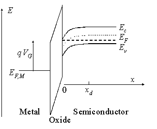
I front a louder band and in the past I would get decently drunk before we went on, I got a bit of a reputation for being (playfully) chaotic on stage, shows either went really well or were total train wrecks. (Think: The Replacements) I’ve quit drinking and haven’t played since, I’m not nervous about playing but I’m kinda nervous about capturing the same energy. So, sober front people, what do you like to do before a show to get yourself hyped up and in the zone? Coffee? Energy drinks? Breath... Energy band bending is changes in energy offset (level) of semiconductor's band structure near junction due to space charge. 2. Depletion layer: In depletion region, voltage applied to gate is greater than flat band voltage and less than threshold voltage. Fig2 energy band diagram and MOSFET internal charge distribution in depletion region
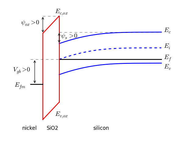
Flat band is the condition where the energy band (E c and E v) of the substrate is flat at the Si-SiO 2 interface as shown in Fig. 5-4. This condition is achieved by applying a negative voltage to the gate in Fig. 5-3b, thus raising the band diagram on the left-hand side. (See Section 2.4 for the relation between voltage and the band ...
Mosfet energy band diagram
The energy band diagram contains the electron energy levels in the MOS structure as deliniated with the fermi energy in the metal and semiconductor as well ...0 votes: MOS capacitor is an equilibrium device i.e. when the external voltage is not applied to the device the Fermi level of metal and semiconductor are ... Transcribed image text: For an N-MOSFET (n-p-n junctions), a) Draw energy band diagram across the device at equilibrium. b) Draw band diagram of the N-MOSFET, under negative gate voltage, and c) Draw band diagram of the N-MOSFET, under high positive gate voltage. 1) Energy band diagrams provide a qualitative understanding of how MOSFETs operate. 23 . 2) MOSFETs are barrier controlled devices - the drain current is controlled by the height of an energy barrier between the source and channel. Lundstrom: 2018 3) In a well-designed transistor, the height of the energy
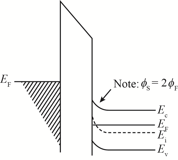
Mosfet energy band diagram. The figure given below shows the combined energy band diagram of MOS system. As shown in this figure, the fermi potential level of metal gate and semiconductor (Si) are at same potential. Fermi potential at surface is called surface potential Φ S and it is smaller than Fermi potential Φ F in magnitude. Download scientific diagram | Energy band diagram for the three possible operation regimes of the MOSFET. from publication: Unified compact model for the ballistic quantum wire and quantum well ... The energy band diagram contains the electron energy levels in the MOS structure as deliniated with the fermi energy in the metal and semiconductor as well as the conduction and valence band edge in the oxide and the silicon. - Energy Band Diagrams are a graphical way to describe the energy needed to change the behavior of a material. Module #2 EELE 414 -Introduction to VLSI Design Page 8 Energy Bands • Energy Bands - Quantum Mechanics created the concept of bands to represent the levels of energy that are present at each "state" of an atom.
On the energy band concept, the conductivity of this semiconductor will become zero at room temperature which is shown in the following figure. The intrinsic semiconductor examples are Si & Ge. Intrinsic Semiconductor. In the above energy band diagram, the conduction band is Fundamentals of MOSFET devices ¾MOS capacitor zFigure (fig3) shows the structure of a MOS capacitor zThe corresponding band diagram is shown in figure (fig4) zSilicon dioxide has a 9 eV bandgap zThis results in large band offset relative to silicon Now we are in a position to draw the band diagram of oxide with its conduction band lying bellow the vacuum level by an amount equal to the electron affinity of oxide which is to be equal to 0.9 eV and the valence band lying bellow the conduction band by an amount equal to the band gap energy of oxide which is roughly equal to 9 eV. View Syllabus. From the lesson. Week 3. 3-1 Metal-Oxide-Semiconductor Field Effect Transistors (MOSFETs) 28:59. 3-2 MOSFET IV Equation, Mobility Calculation, Short/Long Channel MOSFET 15:52. 3-3 MOSFET Band Diagram & Operation Mechanism 9:53. 3-4 n-MOSFET Band Diagram 7:24.
The occupancy of the energy bands in a semiconductor is set by the position of the Fermi level relative to the semiconductor energy-band edges. Application of a source-to-substrate reverse bias of the source-body pn-junction introduces a split between the Fermi levels for electrons and holes, moving the Fermi level for the channel further from the band edge, lowering the … The MOSFET: A Barrier-Controlled Device 3.1 Introduction 3.2 Equilibrium energy band diagram 3.3 Application of a gate voltage 3.4 Application of a drain voltage 3.5 Transistor operation 3.6 IV Characteristic 3.7 Discussion 3.8 Summary 3.9 References 3.1 Introduction MOSFET Modeling & Simulation with MATLAB. The MOS capacitor (a) Physical structure of an n+‐ Si/SiO2/p‐Si MOS capacitor (b) cross section (c) the energy band diagram under ... Hello People of Reddit.Please share your wisdom with me, I am interested to learn from your experience. Situation: I have an P90 PDW with stock 1.65 Joules (thats about 425fps on .2g BB) and I want to lower its energy to something in between 0,5 and 0,7 joules of energy (thats about 250-275 fps on .2g BBs) .It has a lot of proper upgrades and it also has a quick spring exchange gearbox, so I can just drop in another (weak) spring to get to that low FPS quite easy.The gearbox already comes with...
Band Diagram Tunnel Field-effect Transistor MOSFET, PNG ...
MOSFET. MOSFET – An introduction; Gradual Channel Approximation: Derivation of I-V characteristics; Substrate bias effect and subthreshold conduction in MOSFET; Short Channel Effects in MOSFET; Compound Semiconductors. Introduction to compound semiconductors; Basics of heterojunctions; Band diagram of heterojunctions; Heterojunctions (contd).
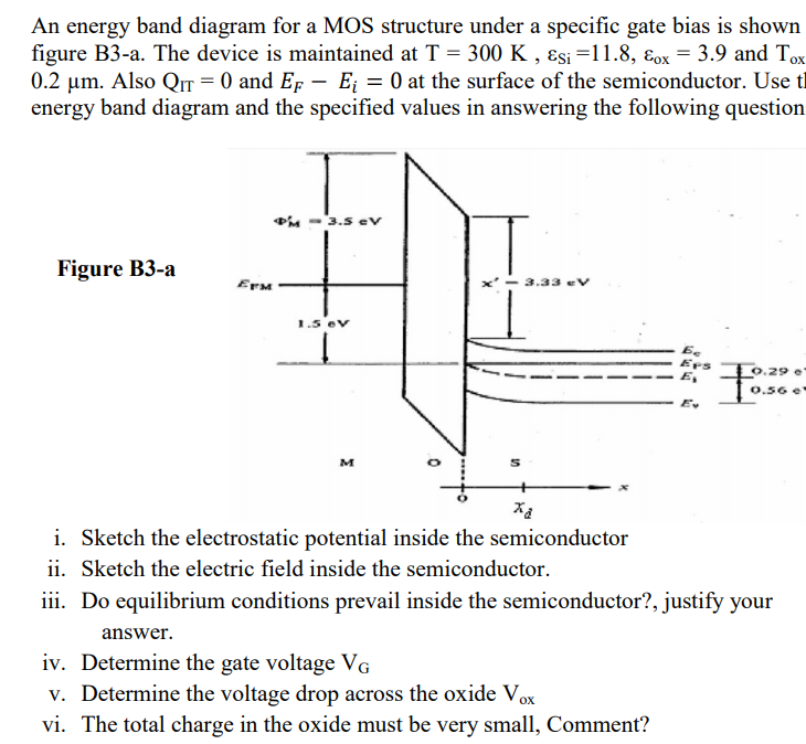
Solved An energy band diagram for a MOS structure under a ...
10.04.2020 · In the previous post on Ideal IV characteristics of MOSFET, we derived the current-voltage relationship assuming a certain number of ideal conditions.But in practical scenarios, there are a lot of non-ideal effects that one needs to keep in mind. In this post, let’s try to get hold of the physical phenomena that cause the non-ideal IV characteristics of a MOSFET.

Charge coupled Device (CCD) | Science 2.0
The energy band diagram of an intrinsic semiconductor is shown below: (a) Intrinsic Semiconductor at T = 0 Kelvin, behaves like an insulator (b) At t>0, four thermally generated electron pairs In intrinsic semiconductors, current flows due …
Impact of band to band Tunneling on Transient performance of ...
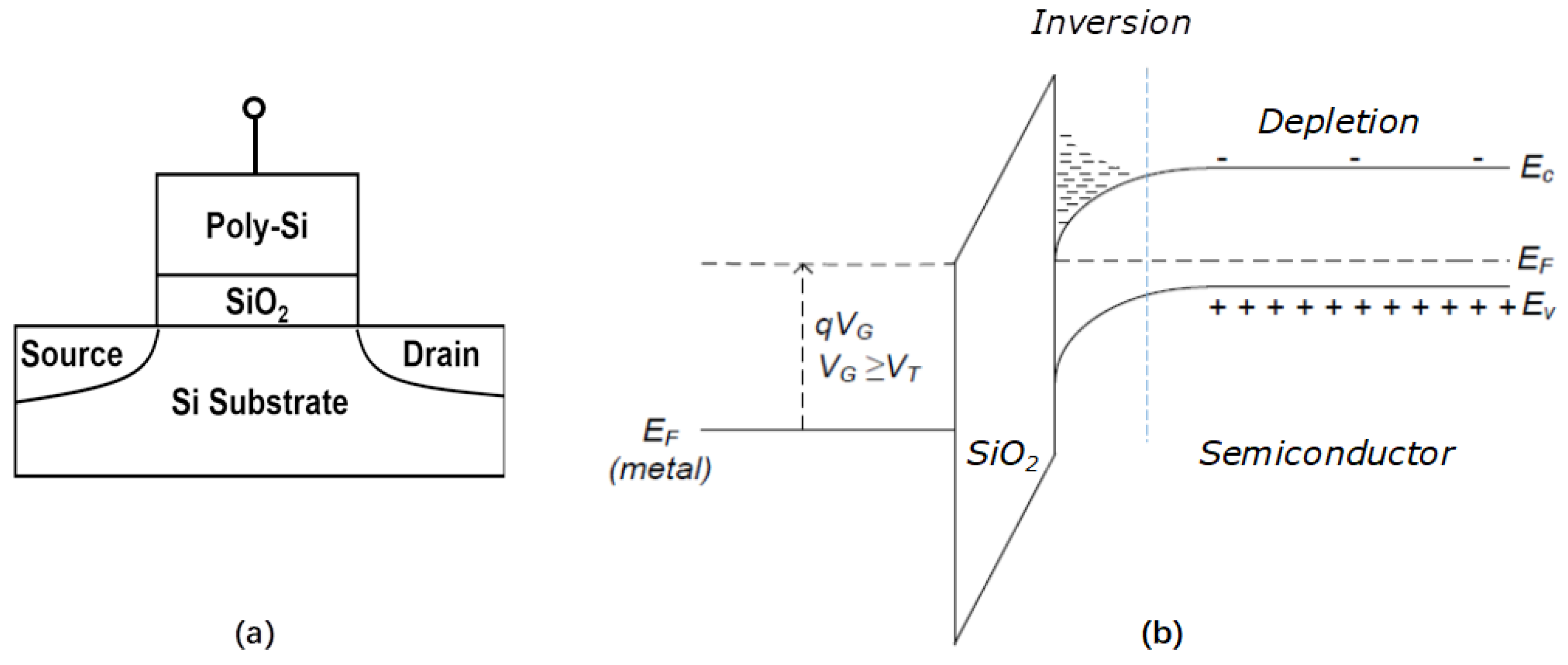
The energy band diagram of the p-type MOS device under inversion condition is shown in Fig. 5.2. Notice that inversion occurred when the surface potential is twice the Fermi potential, which follows equation (5.1). qΦS (inv ) =2qφF (5.1) Figure 5.2: The energy band diagram of p-type MOS device at inversion condition
Fundamentals of Nanotransistors : The MOSFET: A Barrier ...
https://www.patreon.com/edmundsjIf you want to see more of these videos, or would like to say thanks for this one, the best way you can do that is by becomin...
VLSI Design - MOS Transistor
In this module on MOS devices, we will cover the following topics:, MOS device structure, energy band diagram for MOS device at equilibrium, Flat band condition, Accumulation, Depletion, and Inversion of MOS under bias, Energy band diagram and charge distribution for MOS in inversion, Quantitative model and relevant parameters, Energy band diagram with channel bias, Inversion layer charge, and ...
Quantum mechanical compact modeling of symmetric double-gate ...
It seems that I can't wrap my head around the concept of the k-vector and crystal momentum. From my waves course I remember that the wave vector sorta represents where the wave propagates (in an isotropic and homogeneous material). So in solid state that could be thought as the same thing applied to the wave function, right? And here comes the troubles: why and how is it related to the momentum of a particle? I think I get the math behind it but not the concept. Furthermore, given th...

Basic MOS Physics - Power Microelectronics. Device and ...
Hello Pilots, Recently I have been watching the BFM series from "The Air Combat Tutorial Library". In a video (https://youtu.be/rCLywusR3fo), EM diagrams are presented to help better understand an aircraft's performance under certain conditions. These diagrams may also help to understand the strengths and weaknesses an aircraft has when engaged in a dogfight with another type. Does anyone know a place where I can learn how to create EM diagrams? Or maybe a website which generates them for you? ...
Model of MOSFET in Delphi
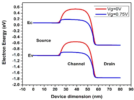
Download scientific diagram | Energy band diagram for an n-channel MOSFET under high gate and drain bias. The current, J , is the thermionic current injected from the 1 from publication: Emission ...

Energy Band Diagram - an overview | ScienceDirect Topics
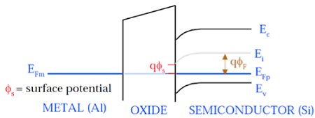
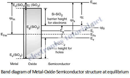
The energy band diagram for ideal MOS capacitor at thermal equilibrium with zero biased voltage condition is shown in Fig. 3.1(b) and (c), whereby E F is the Fermi energy level of metal and semiconductor. E C is the conduction band of the semiconductor. E V is the valence band of the semiconductor, E i is the intrinsic energy level, E VAC
6.4 The Metal-Insulator-Semiconductor FET (MOSFET)(1 ...
Apr 8, 2015 — Now, what effect does a gate voltage have? Lundstrom ECE 305 F15. Page 5. equilibrium energy band diagram. VGS.
Fundamentals of Nanotransistors : The MOSFET: A Barrier ...
Now that I should hopefully be done with internship interviews for the rest of my life, here's a mega list of almost every interview question I was asked from 150+ interviews at Facebook, Apple, Amazon, Nvidia, Google, Microsoft, Qualcomm, Analog Devices, Texas Instruments, Northrop Grumman, SpaceX, Tesla, etc. This is going to be a massive step up from ["part 1"](https://www.reddit.com/r/ECE/comments/iwmpw7/technical_internship_interview_questions_at_big/) that I posted a while back now that I...
![wiki:semiconductors:moscap [Weber's Wiki]](https://hkn.illinois.edu/wiki/_media/wiki:hardware:moscap_accumulation.png)
wiki:semiconductors:moscap [Weber's Wiki]
Metal oxide semiconductor field effect transistor (MOSFET) is an example ... this becomes a MOS structure. It is possible to draw the band diagram for.9 pages

please make cleare hand written Given an ideal p-channel ...
- Energy band diagrams in equilibrium, accumulation, depletion, and inversion modes- MOS capacitor- Charge distributions and electric fields at strong invers...
Introduction to Energy Bands
Fig. 1: Top: Schematic of a tunnel transistor (TFET) architecture; Bottom: Energy band diagram illustrating the TFET ON and OFF state conditions. Quantum Tunneling The Schrödinger formulation of quantum mechanics presents an interesting phenomenon where a particle tunnels through an energy barrier, similar to evanescent wave coupling of electromagnetic waves.

Long Channel MOS Transistors - ppt download
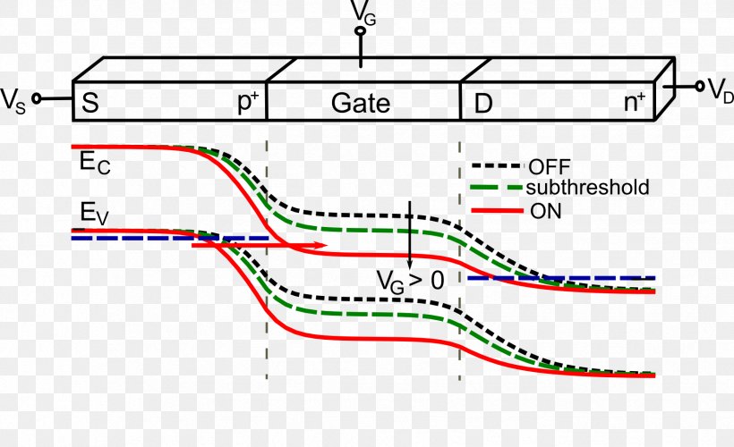
Figure 1. (a) Standard n-MOSFET structure. (b) n-TFET structure in which drain and source doping are no longer symmetrical. (c) Energy band diagram for the n-MOSFET in which current is carried by thermionic emission of electrons. (d) Energy band diagram for
Very large photoresponsiviy and high photocurrent linearity ...
I'm trying to play a melody that I can play on guitar on the harmonica, but I can't find the note, even though it's in the key. I need to find a diagram, but my google searches are useless. Can anyone please help?
VLSI Design - MOS Transistor
c is the energy of the conduction band edge, and E F is the Fermi level at zero applied voltage. The various energies involved are indicated in Figure 1.3, where we show typical band diagrams of a MOS capacitor at zero bias, and with the voltage V = V FB applied to the metal contact relative to the semiconductor-oxide interface.

MOS TRANSISTOR REVIEW
Question 2: 1) Draw the energy band diagram of a MOSFET transistor at equilibrium, when no voltage is applied. [15 marks] 2) When a positive potential is applied to the source contact of a MOSFET transistor, briefly explain what happens to the Fermi level of the source contact and why current flows.
Automated drawing of the MOS band diagram
Energy Band Diagrams Separate ... MOSFET operation - GCA Derivation assumptions are that the transistor is in linear mode: Vgs > Vt (so we have inversion and a channel) Vds < Vgs - Vt (so the channel extends from source to drain) Vbs = 0, so no body effect modifications of the threshold voltage.
Overview of Semiconductor Devices
Band-to-Band Tunneling For small gate bias at high drain bias a significant drain leakage can be observed, especially for short channel devices. The electric field can be very high in the drain region for VD high and VG = 0. This can cause band-to-band tunneling. This will happen only if the electric field is sufficiently high to cause large ...
Solved: Chapter 17 Problem 3P Solution | Semiconductor Device ...
So Im just at the start of the game and I’m currently producing 30 megawatts of energy. People who just have all planets in one sytems full with machines. How much Megewatts are you producing and using right now?

MOSFET Band Diagram Explained
Energy Diagram of P-type Semiconductor. The p-Type Semiconductor energy band diagram is shown below. The no. of holes within the covalent bond can be formed in the crystal by adding the trivalent impurity. A less amount of electrons will also be accessible within the conduction band. Energy Band Diagram

SSPD_Chapter 6_Part 4_concluded_MOS Physics
2D energy band diagram on n-MOSFET Lundstrom ECE 305 F16 (a) (b) (c) (d) S.M. Sze, Physics of Semiconductor Devices, 1981 and Pao and Sah. a) device b) equilibrium (flat band) c) equilibrium (ψ S > 0) d) non-equilibrium with V G and V D > 0 applied F N 22

Lecture 15 OUTLINE The MOS Capacitor Energy band
1) Energy band diagrams provide a qualitative understanding of how MOSFETs operate. 23 . 2) MOSFETs are barrier controlled devices - the drain current is controlled by the height of an energy barrier between the source and channel. Lundstrom: 2018 3) In a well-designed transistor, the height of the energy

Figure 6 from Hot-carrier effects in Hydrogen-passivated p ...
Transcribed image text: For an N-MOSFET (n-p-n junctions), a) Draw energy band diagram across the device at equilibrium. b) Draw band diagram of the N-MOSFET, under negative gate voltage, and c) Draw band diagram of the N-MOSFET, under high positive gate voltage.

Energy band diagrams of a) M1 & b) M2 MOS capacitors with no ...
The energy band diagram contains the electron energy levels in the MOS structure as deliniated with the fermi energy in the metal and semiconductor as well ...0 votes: MOS capacitor is an equilibrium device i.e. when the external voltage is not applied to the device the Fermi level of metal and semiconductor are ...
MOSFETs: An Energy Band Treatment

Energy band diagram for the three possible operation regimes ...
Band-Diagram-of-Ideal-MOS | MOS-Capacitor Digital-CMOS-Design ...
MOS Capacitors
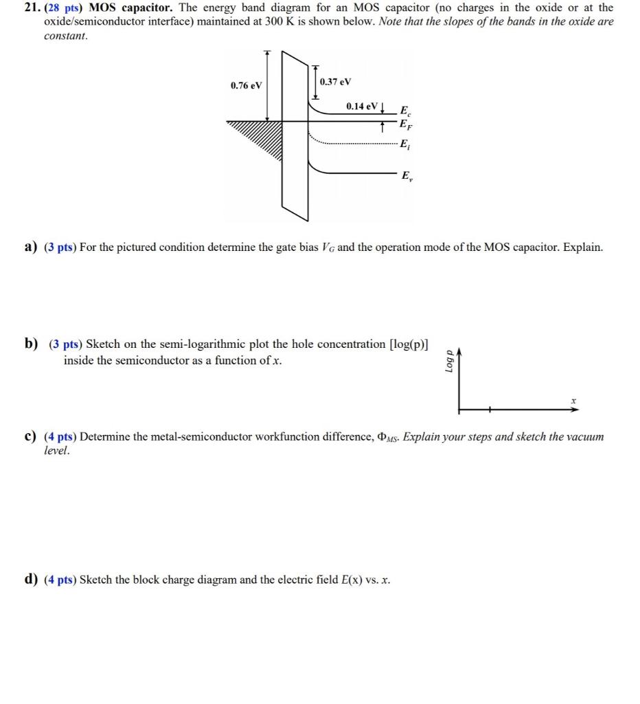
21. (28 pts) MOS capacitor. The energy band diagram | Chegg.com
Lecture 14: MOSFETs

The MOS capacitor. (a) Physical structure of an n+-Si/SiO2/p ...

What is the concept of 'flat band voltage' in MOSFET devices ...

Energy band diagram of an MOS capacitor and operating regions ...
Week12HW SolutionsV2
Applied Sciences | Free Full-Text | Atomic Layer Deposition ...

Draw and explain energy band diagram of MOS capacitor in ...
0 Response to "39 mosfet energy band diagram"
Post a Comment