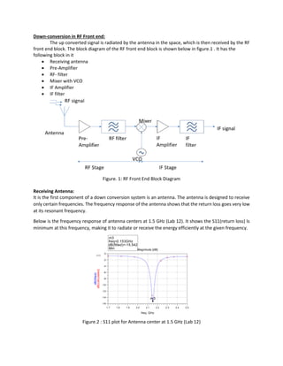
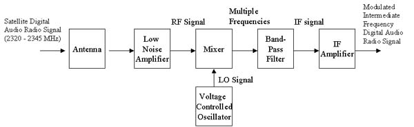
42 rf front end block diagram
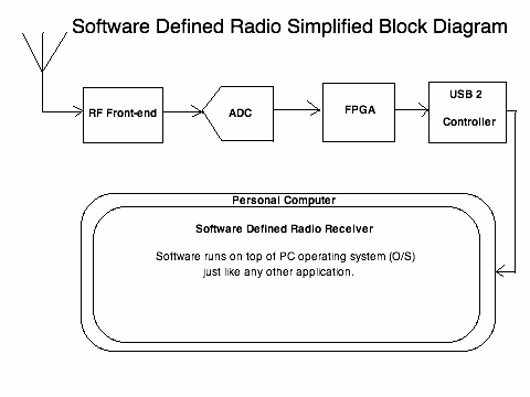
USRP B200mini-i | Ettus Research, a National Instruments ... The USRP™ B200mini-i delivers a 1x1 SDR/cognitive radio in the size of a business card. With a wide frequency range from 70 MHz to 6 GHz and a user-programmable, industrial-grade Xilinx Spartan-6 XC6SLX75 FPGA, this flexible and compact platform is ideal for both hobbyist and OEM applications. The RF front end uses the Analog Devices AD9364 RFIC transceiver with 56 MHz of instantaneous ... RF Front End - ShareTechnote RF Front End · The antenna(s) and antenna tuner(s) · Band Select, Duplexers: filters, duplexers, diplexers, and switches used for frequency control · Transmitters ...
PDF GPS front-end components - Infineon Technologies Below is a general block diagram for GPS functionality in a device. From the antenna looking into GPS receiver, the ESD device protects the RF front-end against ESD hazards coming from ANT when it makes contact with the external environ-ment. In modern wireless handheld systems, 8 kV contact dis-

Rf front end block diagram
RF Front End Receiver System Design for 5G Applications Block Diagram of Receiver RF Front End. Oscillators are found in all most every modern wireless communications, radar and remote sensing ... GPS front-end block diagram - Electronic Products BGU7003 and BGU7005 LNAs. Optimized for small footprint and flexibility, the BGU7003 is ideal for GPS front-end modules. The BGU7005, optimized for a minimum of non-critical external components, is an excellent solution for discrete implementations of the GPS front-end. Both products have an enable function. 5G Cell Phone Block Diagram - RF Wireless World The figure-2 depicts basic block diagram of 5G cell phone architecture. As shown the architecture include baseband part, digital RF interface such as DigRF, ADC/DAC and RF Transceiver. The basic components are same in the 5G phone except antenna array is used instead of one antenna to support massive MIMO and beamforming.
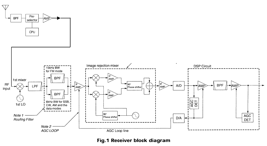
Rf front end block diagram. PDF LTE RF Front-End Architecture 2 LTE RF Front-End Design Challenges ... As shown in the simplified diagram below, the key front end components are power amplifiers (PA) and transmit/receive path or duplex filters and switches for band selection or antenna switch module. Figure 1. Simplified Front -End Block Diagram . From UMTS to LTE and beyond, the RF component technologies ... RF front end - Wikiwand Block diagram of a superheterodyne receiver. The RF front end consists of the components on the left colored red. In a radio receiver circuit, the RF front ... Complete Stand-Alone GPS Receiver Solutio - Maxim Integrated Figure 1 shows the important building blocks and features of Maxim's complete GPS RF solution. Description of the building blocks can be found in Table 1; cascaded performances are shown in Table 2. Figure 2 shows the application circuit of the GPS receiver RF portion with the MAX2742. Figure 1. GPS RF front-end block diagram. Table 1. How Do New Wireless Protocols Like Wi-Fi6E Affect RF Front-End ... RF front ends are one of the most important hardware blocks involved ... Block diagram of the SKY85784-11, a new Wi-Fi6E front-end module.
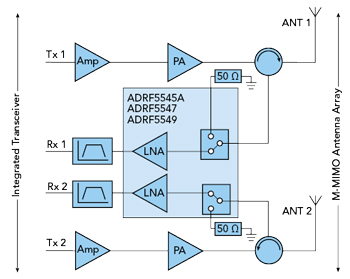
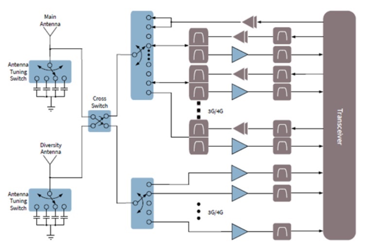
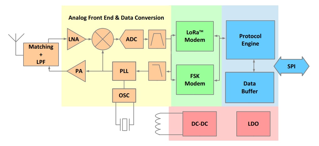
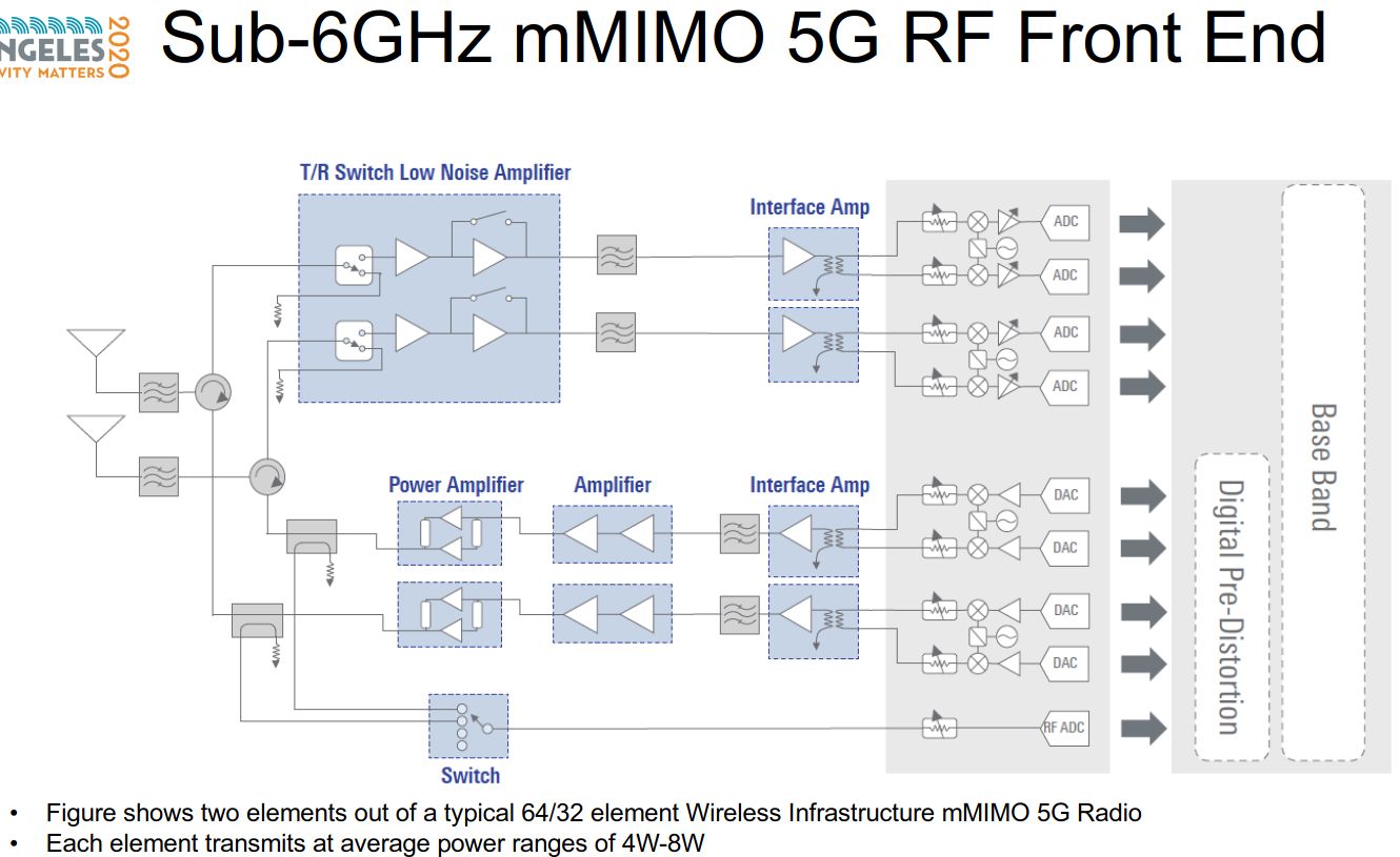
PDF Multi-band Sub-GHz RF Front End - Mouser Electronics Figure A: SX1250 Block Diagram General Description The SX1250 is a sub-GHz RF Front End device designed to work along with Semtech's SX1302 baseband engine, to design a high-performing LoRa® or LoRaWAN gateway. It covers any frequency band below 1 GHz, making it the perfect candidate to support any license-free band used in today's IOT use cases. ADI's RF Front-End Family Enables Compact 5G Massive MIMO ... An ADRF5545A/ADRF5547/ADRF5549 application block diagram for a M-MIMO RF front-end design is shown in Figure 1. The device has channels that incorporate a high power switch followed by a two stage LNA. During receive mode operation of the transceiver, the switch routes the input signal to the LNA input. RF generic front-end block diagram - Electronic Products RF generic front-end block diagram Posted on January 6, 2014 by Electronic Products In virtually every wireless application from mobile or networking infrastructure (W-LAN / ISM / RFID), through fixed wireless and industrial applications including e-metering there is always a demand to improve basestation performance. Basestations PDF Mobile Phone RF Front End Integration Roadmap Front End Block Diagram CA the Three Bands LB -699 to 960 MHz MB -1428 to 2170 MHz HB -2300 to 2690 MHz J. Young "arrier Aggregation, Quantifying Front End Losses," IWPC Chicago Meeting Sept. 16, 2014 2, 3, 4G Module LB GGE MB GGE B1 B4 B25 B3 B8 B20 B26 B12 PA Bias and Control MIPI Interface Switch Bias and Control Load
Simplified block diagram of the RF front-end. - ResearchGate Fig.1 is a simplified block diagram of the proposed RF front-end that is based on the previous work presented in [1]. The first stage of ... (a) Simplified block diagram of the RF front-end. (b ... Download scientific diagram | (a) Simplified block diagram of the RF front-end. (b) Frequency plan. from publication: A 900-MHz transceiver chipset for two-way paging applications | A 900-MHz ... Detection and Measurement of Radar Signals: A Tutorial diagram, the minimum decibel amount of attenuation, A, required will be: (B-1) where Aext = external attenuation (dB) as shown in Figure 1 Pp = peak power produced by the radar transmitter (dBm) Lc = loss through the coupler (dB) Ain = attenuation provided internally at the measurement device front end input (dB) Dual-Channel, 3.3 GHz to 4.0 GHz, 20 W Receiver Front End ... The ADRF5515 is a dual-channel, integrated RF, front-end, multichip module designed for time division duplexing (TDD) applications. The device operates from 3.3 GHz to 4.0 GHz. The ADRF5515 is configured in dual channels with a cascading, two-stage, LNA and a high power silicon SPDT switch. In high gain mode, the cascaded two-stage LNA and switch
RF front-end Group
Block 1: RF Front End - Academics | Bradley University Figure 3: Sub-Level Block Diagram Block 1: RF Front End. A RF signal is input into the RF front end as shown in Figure 4. In lab, a signal generator produces the RF signal, but in application, an antenna would be used to receive the signal. The signal is amplified in a low-noise amplifier (LNA) to increase the power of the input signal.
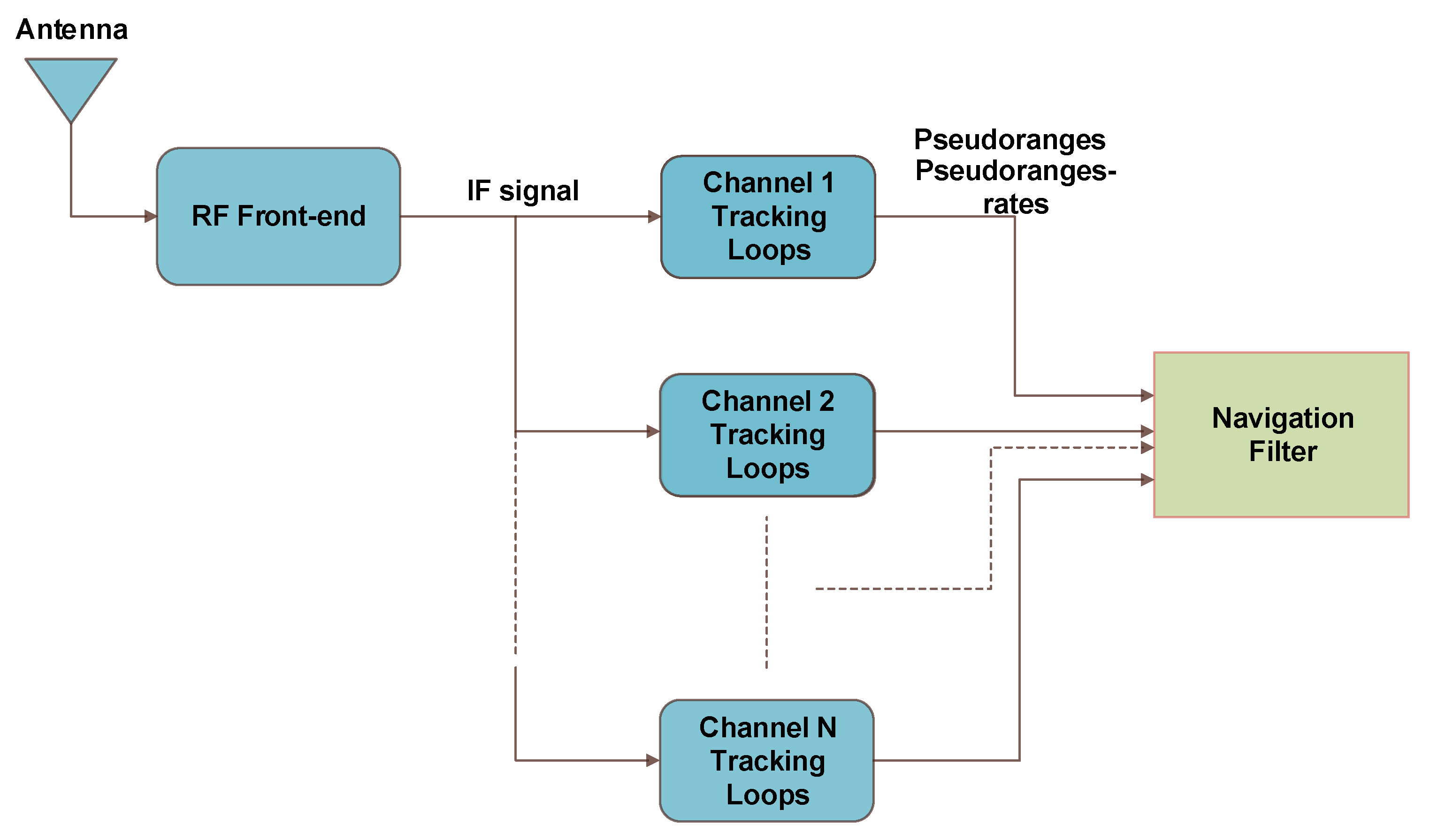
Applied Sciences | Free Full-Text | An Efficient Ultra-Tight ...
PDF Electronic Warfare Digital Radar Receiver - Bradley Figure 3: Sub-Level Block Diagram Block 1: RF Front End A RF signal is input into the RF front end as shown in Figure 4. In lab, a signal generator produces the RF signal, but in application, an antenna would be used to receive the signal. The signal is amplified in a low-noise amplifier (LNA) to increase the power of the input signal.
The Changing Face of the Power Amplifier in 5G Radios ...
PDF RF Front End Module Architectures for 5G Fig. 1. 4G/5G RF front end diagram. • Improve the power efficiency for mmWave FR2 radios; most probably FR2 will be used mainly for downlink in mobile applications [10, 11]. • Increase the number of antennas to 6-8 with the requirement to reach these antennas from different 4G/5G LTE radios which have to coexist with multiple
Circuit Design (GPS) Part 1
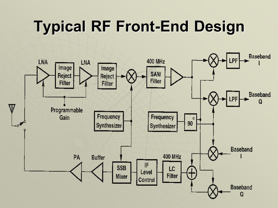
RF Front End Design: Specifications and Component ... The functional block diagram below shows the general topology of an RF front end. Here, we've lumped the Tx and Rx sides together using an antenna switch, which allows an incoming/outgoing signals to be routed on the Rx/Tx sides of the signal chain, respectively.
Introducing The Most Advanced SDR – The NI Ettus USRP X410 ...
Superheterodyne receiver - Wikipedia RF front end Refers to all the components of the receiver up to and including the mixer; all the parts that process the signal at the original incoming radio frequency. In the block diagram above the RF front end components are colored red. See also. H2X radar; Automatic gain control; Demodulator; Direct conversion receiver; VFO

Complete Stand-Alone GPS Receiver Solution with MAX2742
PDF Design of Reconfigurable Radio Front-Ends Design of Reconfigurable Radio Front-Ends Xiao Xiao Electrical Engineering and Computer Sciences University of California at Berkeley Technical Report No. UCB/EECS-2018-142
ShareTechnote
RapidRF LDMOS Front-End Designs | NXP Semiconductors RapidRF Front-end Design. NXP's RapidRF front-end designs for 5G infrastructure integrate a linear pre-driver, RF power amplifier, Rx LNA with T/R switch, a circulator and a bias controller in a compact footprint. They incorporate a coupler for DPD feedback and are to be used with digital pre-distortion.

RTL-SDR Front End Scicos Simulation – Telecommunications ...
RF Agile Transceiver Data Sheet AD9363 - Analog Devices The AD9363 is a high performance, highly integrated RF agile transceiver designed for use in 3G and 4G femtocell applications. Its programmability a nd wideband capability make it ideal for a broad rang e of transceiver applications. Th e device combines an RF front end with a flexible mixed-signal baseband section and
lab_13_14_essay
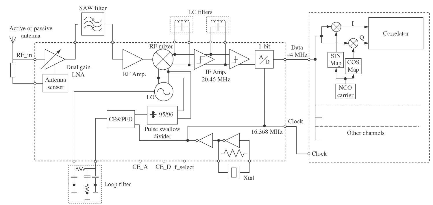
Developing a UHF RFID Reader RF Front End with an Analog ... A UHF RFID reader RF front end using an AD9361 block diagram. The AD9361 transmitter monitor path gain distribution is comprised of two gains: front-end gain (transmitter monitor gain) and receive low-pass filter gain (G BBF ). The transmitter monitor gain could be set to 0 dB, 6 dB, or 9.5 dB. G BBF could be set from 0 dB to 24 dB with 1 dB step.

RFbeam
Block diagram of the RF front-end module - ResearchGate Block diagram of the RF front-end module ... As wireless communication devices become smaller and lighter, less space is allowed for the placement of the RF ...

ADI's RF Front-End Family Enables Compact 5G Massive MIMO ...
Qualcomm 315 5G IoT Modem | Qualcomm Enabling up to 50% smaller modules than existing 5G modules that involves a reduced chipset footprint with highly integrated RF front-end. Qualcomm 315 is purposely designed to provide a pin-to-pin compatible solution for current LTE legacy modules and provides for a seamless transition from LTE to 5G.
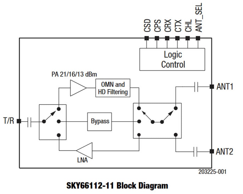
SKY66112-11 RF Front End Module - Skyworks Solutions Inc ...
Home | Guerrilla RF 5G TDD mMIMO Block Diagram. 5G FDD mMIMO Block Diagram. ... GPS/GNSS Front End Solutions. SHARK FIN - SDARS FRONT END ... Founder and CEO of Guerrilla RF.
Some Thoughts on the IC-7800 Front End
PDF RF Front-End Challenges for Joint Communication and Radar ... RF Front-End Challenges for Joint Communication and Radar Sensing ... padmanava.sen, andre.nollbarreto, gerhard.fettweis@barkhauseninstitut.org Abstract—In this paper, radio-frequency (RF) hardware challenges for joint communication and radar sensing (JC&S) applications are studied. ... shows the block diagram of a typical Fig. 2: Chirp-based ...

CML front end IC bridges RF and DSP
RF Front End | Multimode, Multiband RF | Qualcomm Qualcomm Technologies offers an extensive RF Front End portfolio engineered to deliver integrated solutions for industry-leading RF performance. Our portfolio of power amplifier modules, front-end modules, and diversity receive modules is designed to support virtually all sub-6 GHz and mmWave bands in highly integrated configurations, while ...

RF generic front-end block diagram - Electronic Products
Solved [50 points] A dual-band radio handset has an RF ... Transcribed image text: [50 points] A dual-band radio handset has an RF receiver front-end block diagram such as the one shown below IF Mixer I-Channel Antenna Receiver Front-End Mixerl Buffer Lowpass Filters Duplexer RF ilter RFLNA Image Reject FilterAmp Amp Filter LO 5 6 Q-Channel Each stage in this receiver is given a number and the table below contains the specifications for each component ...
The Ham Radio Receiver Of Tomorrow Is Here
Modeling RF Front End in Radar System Simulation - MATLAB ... Modeling RF Front End in Radar System Simulation. In a radar system, the RF front end often plays an important role in defining the system performance. For example, because the RF front end is the first section in the receiver chain, the design of its low noise amplifier is critical to achieving the desired signal to noise ratio (SNR).

Block diagram of RF front-end for terrestrial DTV tuner ...
PDF 2.4-GHz RF FRONT END - TI high performance RF front end for low-power and low-voltage wireless applications in the 2.4-GHz band. Its single-ended RF input and output make it compatible with any manufacturer's transceiver if appropriate external parts are used. When a transmit/receive (T/R) switch and a balun are used, it can interface with existing and

RF Front End Design: Specifications and Component Selection ...
RF front-end - Infineon Technologies RF front-end solutions from Infineon. As a leading provider with over 60 years experience developing RF front-end solutions, Infineon offers you a broad product portfolio of high performance RF front-end components. Choose our innovative solutions and benefit from speedy, reliably delivery as well as our in-depth system knowledge and on-site ...
RF Front-End Family Enables Compact 5G Massive MIMO Network ...
Module Introduction - NXP Label the components of a generic radio block diagram. – Explain the path that an RF signal ... They are used extensively in the front end of a radio.
Wireless Transceiver RF Front-Ends An overview of the main ...
Superheterodyne Receiver: Block Diagram » Electronics Notes RF tuning & amplification: This RF stage within the overall block diagram for the receiver provides initial tuning to remove the image signal. It also provides some amplification. There are many different approaches used within the RF circuit design for this block dependent its application. The electronic circuit design presents some challenges.

25382592EM The CC2538-CC2592EM is a development tool for TIs ...
Developing a UHF RFID Reader RF Front End - Semiconductor ... A UHF RFID reader RF front end using an AD9361 block diagram. The AD9361 transmitter monitor path gain distribution is comprised of two gains: front-end gain (transmitter monitor gain) and receive low-pass filter gain (GBBF). The transmitter monitor gain could be set to 0 dB, 6 dB, or 9.5 dB. GBBF could be set from 0 dB to 24 dB with 1 dB step.

NCx3321| Automotive NFC Frontend | NXP Semiconductors
Block Diagrams for RF and Microwave Systems - Pasternack Pasternack's library RF and microwave block diagram are designed to provide engineers and designers with examples of common RF systems schematics while illustrating the RF products and where they fit into the system's design.
RF front-end block diagram | Download Scientific Diagram
LabVIEW Front Panel Explained - NI Feb 04, 2020 · The front panel has controls and indicators, which are the interactive input and output terminals, respectively, of the VI. Controls and indicators placed on the front panel are automatically placed on the block diagram. Refer to the “Block Diagram” tutorial for more information on block diagram terminals.
Infineon - BGSC2341ML10 -RF digitally tunable capacitor + ...
What is an RF Front End (RFFE)? | OnScale The RF Front end is the generic name for all the circuitry between a receiver Antenna input up to the Mixer Stage. For most architectures, the RF Front End consists of: An RF Filter (which is actually a band-pass filter) receives the Electromagnetic wave from the Antenna. His role is to remove the image frequency and to prevent strong out-of ...

EETimes - A Slow Penetration for RF CMOS
VME Bus Description, Pinout and VME Standards information VME Bus Description The VME bus is a scalable backplane bus interface. VME Cards may be produced which respond to the following Address widths or Data widths: A01 - A15, A01 - A23, A01 - A31, or A01 - A40 D00 - D07, D00 - D15, D00 - D23, D00 - D31, or D00 - D63 (undefined before Rev. C).
Design of RF Front End for Multi-Band Multi-System GNSS ...
RF front end - Wikipedia From Wikipedia, the free encyclopedia Block diagram of a superheterodyne receiver. The RF front end consists of the components on the left colored red. In a radio receiver circuit, the RF front end, short for radio frequency front end, is a generic term for all the circuitry between a receiver's antenna input up to and including the mixer stage.

RF Front End Design: Specifications and Component Selection ...
A Multi-Cell Front-End for Longer Battery Life Mar 11, 2022 · The Battery Front End is one of the most important components of a BMS, as it is responsible for monitoring the battery status and operating environment on a regular basis, optimizing battery life and preventing catastrophic failures. As the voltage and number of cells in Li-ion batteries rise, this component becomes increasingly significant. A ...

Simplified ASIC front end block diagram | Download Scientific ...
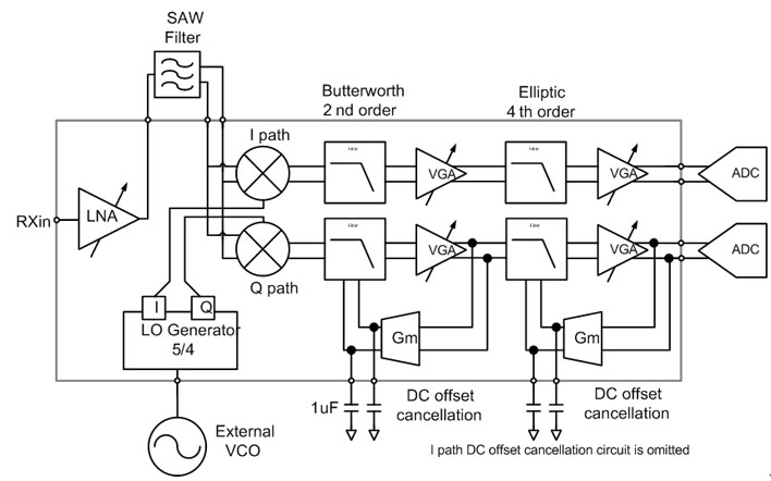
Block diagram of the designed RF tuner. | Download ... Block diagram of the designed RF tuner. ... In the RF front-end, a RF input signal is amplified by a low noise amplifier and G_m with configurable gain steps (41/35/29/23 dB) with optimized noise ...

Developing a UHF RFID Reader RF Front End with an Analog ...
5G Cell Phone Block Diagram - RF Wireless World The figure-2 depicts basic block diagram of 5G cell phone architecture. As shown the architecture include baseband part, digital RF interface such as DigRF, ADC/DAC and RF Transceiver. The basic components are same in the 5G phone except antenna array is used instead of one antenna to support massive MIMO and beamforming.

WiFi and Bluetooth® Connectivity Solutions – Skyworks | DigiKey
GPS front-end block diagram - Electronic Products BGU7003 and BGU7005 LNAs. Optimized for small footprint and flexibility, the BGU7003 is ideal for GPS front-end modules. The BGU7005, optimized for a minimum of non-critical external components, is an excellent solution for discrete implementations of the GPS front-end. Both products have an enable function.

MITSUBISHI ELECTRIC CORPORATION ITAMI WORKS K band RF front ...
RF Front End Receiver System Design for 5G Applications Block Diagram of Receiver RF Front End. Oscillators are found in all most every modern wireless communications, radar and remote sensing ...
SX1250 Multi-band Sub-GHz RF Front End - Semtech | Mouser

Design the Best Front End for UHF Partial Discharge Online ...

Low‐power 2.4 GHz ZigBee transceiver with inductor‐less radio ...
ShareTechnote
IMS 5G Summit: Design challenges remain (part 1) - 5G ...

1 Simplified RF front end transceiver block diagram ...

MAX2745 Single-Chip Global Positioning System Front-End ...

RF Technical Notes - Transmitter Output Factors
Simplified block diagram of the RF front-end. | Download ...

Das 4G- und 5G-RF-Front-End verfügt über Quad-DAC und Quad ...
Functional Description
0 Response to "42 rf front end block diagram"
Post a Comment