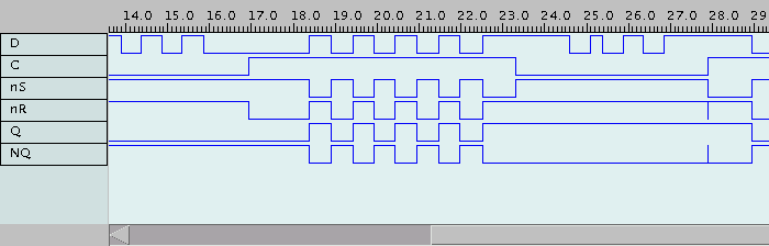
38 d latch timing diagram
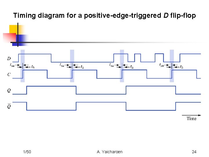
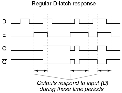
D Type Flip-flops · Operation. · The Data Latch · Ripple Through · The Edge Triggered D Type Flip-flop · Synchronous and Asynchronous Inputs · Timing Diagram · The D ... In the first timing diagram, the outputs respond to input D whenever the enable (E) input is high, for however long it remains high. When the enable signal ...
timing diagram and structure of transparent latch are reviewed, with traditional latch delay model. A new point of view for latch working mode based on a 3-D analysis is proposed in Section III. Section IV presents our new latch delay model taking into account variations such as data slew, clock slew among others Statistical timing analysis for
D latch timing diagram
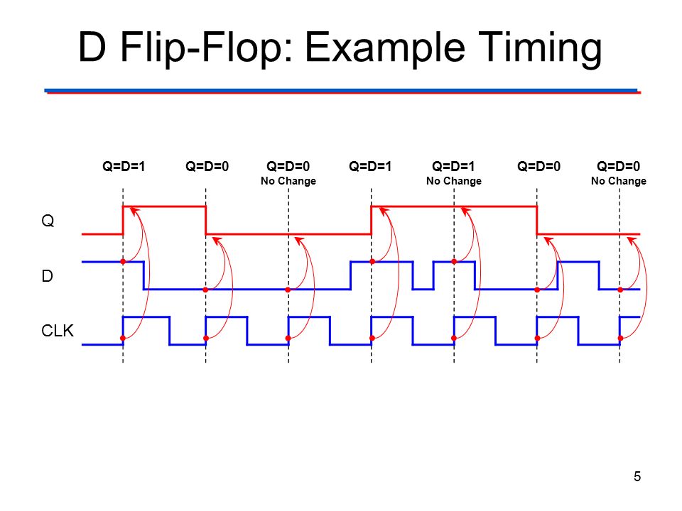
D Q CLK Positive Latch 0 1 D Q CLK ... (less aggressive, recommended timing) FSM clk Q D address read_data write_data Control (write, read, reset) Data[7:0] Address[12:0] W G E1 SRAM V DD E2 W_b G_b ext_address ext_data D Q int_data D Q data_oen address_load data_sample write states 1-3 write completes Q. (a) Circuit. (b) Timing diagram. Timing diagrams. T flip-flops and SR latches. 2. CSE, Lecture The D latch. Output depends on clock. Clock high: Input passes to output. Clock . Flip-flops, D-type flip-flops explained, Data latch, ripple-though, edge-triggering, synchronous and Timing Diagram for a Level Triggered D Type Flip-flop. A D Flip Flop (also known as a D Latch or a ‘data’ or ‘delay’ flip-flop) is a type of flip flop that tracks the input, making transitions with match those of the input D. The D stands for ‘data’; this flip-flop stores the value that is on the data line. It can be thought of as a basic memory cell. In an active high SR Flip Flop is ...
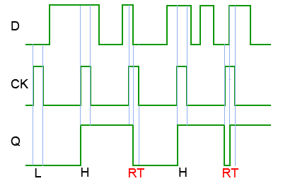
D latch timing diagram. The Gated D Latch Timing Diagram. February 6, 2012 ECE 152A - Digital Design Principles 28 The Edge Triggered D Flip-Flop D Q DQ sample edge Clk D Q. M Horowitz EE 371 Lecture 6 12 Latch Timing • Setup and hold times are defined relative to the clock fall – Setup time: how long before the clock fall must the data arrive – Hold time: how long after the clock fall must the data not change Timing diagrams. □ T flip-flops and SR latches. 2. CSE370, Lecture 14. The D latch. ◇ Output depends on clock. □ Clock high: Input passes to output. Timing diagram. From the timing diagram it is clear that the output Q changes only at the positive edge.At each positive edge the output Q becomes equal to the input D at that instant and this value of Q is held untill the next positive edge . Characteristics and applications of D latch and D Flip Flop : 1.
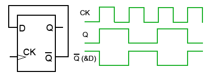
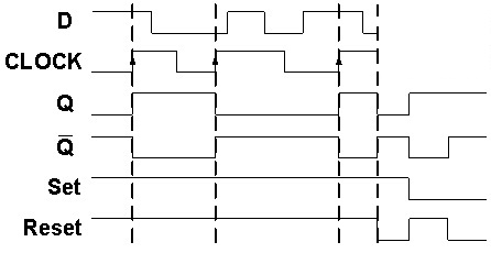
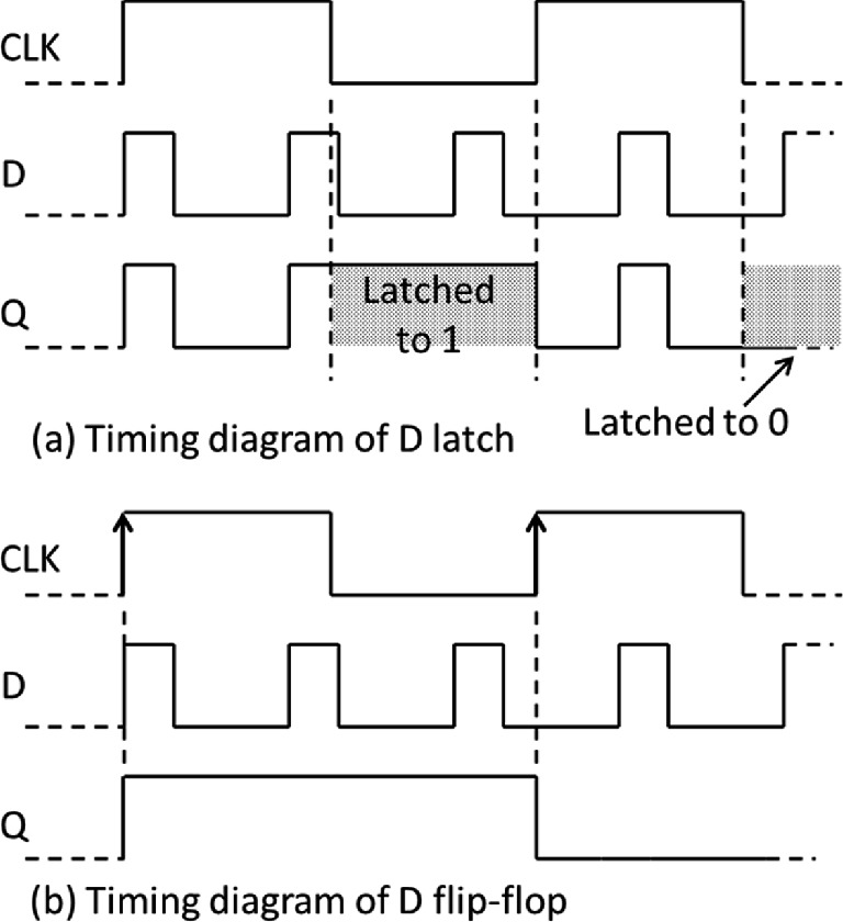
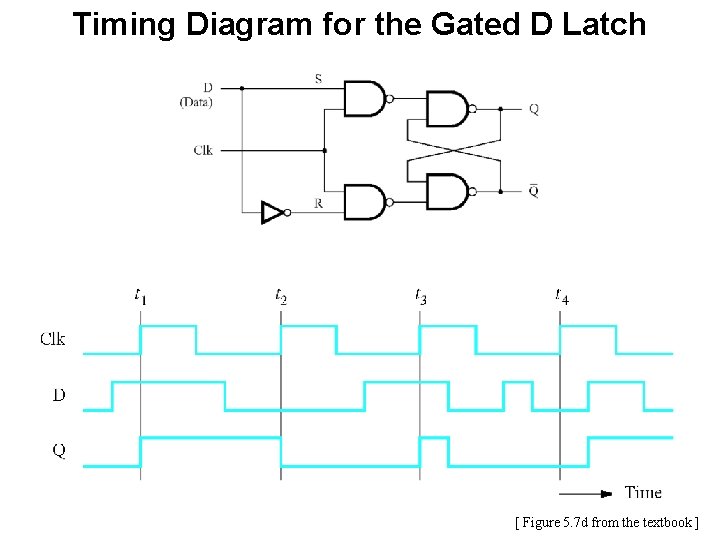
A timing diagram for the D latch is shown below in Fig. 4. Note that when the Gate input is asserted, the output Q simply follows the input. But when the Gate input is not asserted, the output remembers the value present at D at the time the Gate signal was de-asserted. Figure 4. D-Latch timing. Timing diagram for D flop are explained in this video, if you have any questions please feel free to comment below, I will respond back within 24 hrs " Timing diagrams 2 The D latch! Output depends on clock " Clock high: Input passes to output " Clock low: Latch holds its output! Latch are level sensitive and transparent DQ Q CLK Input Output Output CLK D Qlatch CSE370, Lecture 153 The D flip-flop! Input sampled at clock edge A D Flip Flop (also known as a D Latch or a ‘data’ or ‘delay’ flip-flop) is a type of flip flop that tracks the input, making transitions with match those of the input D. The D stands for ‘data’; this flip-flop stores the value that is on the data line. It can be thought of as a basic memory cell. In an active high SR Flip Flop is ...
Q. (a) Circuit. (b) Timing diagram. Timing diagrams. T flip-flops and SR latches. 2. CSE, Lecture The D latch. Output depends on clock. Clock high: Input passes to output. Clock . Flip-flops, D-type flip-flops explained, Data latch, ripple-though, edge-triggering, synchronous and Timing Diagram for a Level Triggered D Type Flip-flop. D Q CLK Positive Latch 0 1 D Q CLK ... (less aggressive, recommended timing) FSM clk Q D address read_data write_data Control (write, read, reset) Data[7:0] Address[12:0] W G E1 SRAM V DD E2 W_b G_b ext_address ext_data D Q int_data D Q data_oen address_load data_sample write states 1-3 write completes
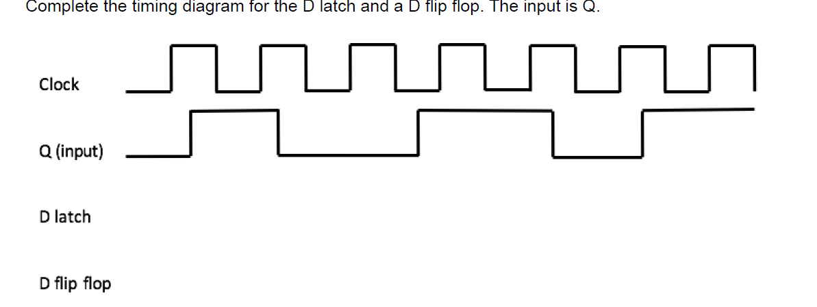
Solved Complete The Timing Diagram For The D Latch And A D Chegg Com

Latch Vs Flip Flop Difference Between Latch And Flip Flop
D Type Flip Flops
D Type Flip Flops
D Type Flip Flops
Flip Flops And Latches Ppt Video Online Download
Flipflops Basic Concepts 150 A Yaicharoen Flipflops N
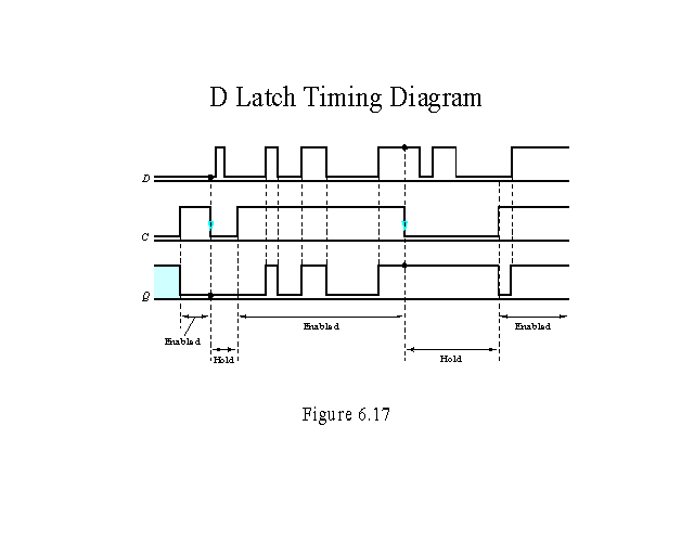
D Latch Timing Diagram
Homework 5 With Solutions Homework Eecs 31 Cse 31 Ics 151 Daniel D Gajski S Web Site

A Divide By 2 Prescaler And B Timing Diagram 3 2 2 3 Prescaler Download Scientific Diagram

Flip Flop Electronics Wikipedia
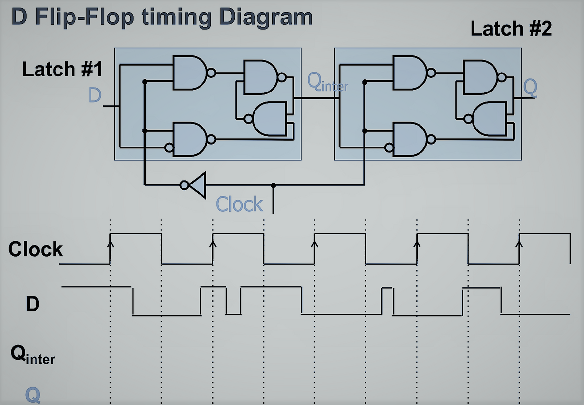
D Type Latch With Nand Gates

A 5 Marks Explain The Difference Between A Latch A Gated Latch And A Flip Flop Homeworklib
Designing Of D Flip Flop
People Ee Duke Edu

D Latch Delay D Latch A Logic Symbol

D Flip Flop Timing Diagram Slide Share

Timing Diagram For An Asynchronous D Flip Flop Youtube
De Preferat Claritate Cartofi Level Triggered D Flip Flop Elchefjames Com

D Type Flip Flop Counter Or Delay Flip Flop
Flip Flops And Latches Northwestern Mechatronics Wiki
Latches And Flip Flops Springerlink
Cpr E 281 Digital Logic Instructor Alexander Stoytchev
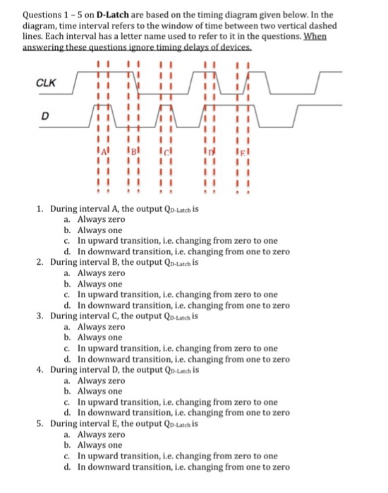
Solved Questions 1 5 D Latch Based Timing Diagram Given Diagram Time Interval Refers Window Time Q34709788 Coursehigh
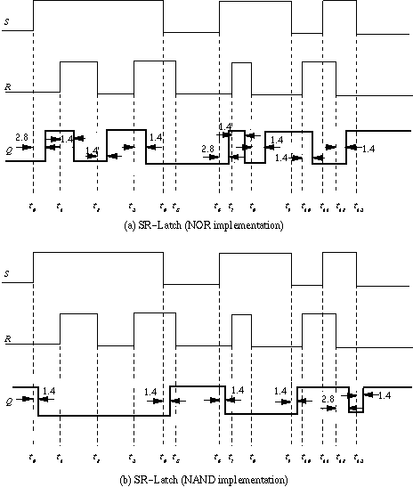
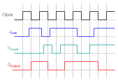
Solved Problem 1 Timing Diagrams 10 Points Bumplete The Timing Diagram For The J Latch And D Ip Flap The Flip Flap Is Positive Edge Triggered Course Hero
Edge Triggered Latches Flip Flops Instrumentationtools
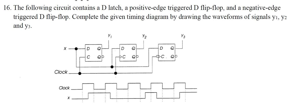
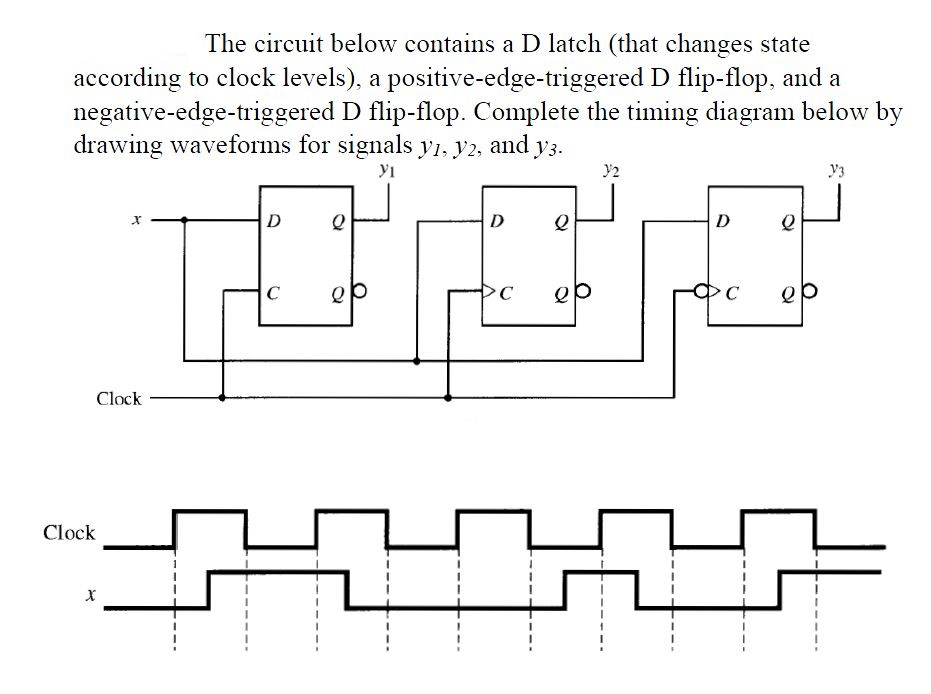
Answered 16 The Following Circuit Contains A D Bartleby

Flip Flop Electronics Wikiwand
1

Master Slave Flip An Overview Sciencedirect Topics

Tutorial Teknik Digital Rangkaian Pencacah Counter Aditya Rizki S Note

Tolgy Asitozas Rutin Flip Flop Timing Diagram L Designer Net
Answered D Flip Flop Timing Diagram Latch 2 Bartleby
Flipflops Basic Concepts Flipflops N A Flipflop Is

Digital Circuits And Systems Circuits I Sistemes Digitals Csd Eetac Upc
20160831 Flip Flop
1

D Type Flip Flop Counter Or Delay Flip Flop
0 Response to "38 d latch timing diagram"
Post a Comment