40 pn junction energy band diagram
1) Introduction to p-n junction transistors 2) Drawing band-diagrams 3) Analytical solution in equilibrium 4) Band-diagram with applied bias Klimeck –ECE606 Fall 2012 –notes adopted from Alam Topic Map 24 Equilibriu m DC Small signal Large Signal Circuit s Diode Schottk y BJT/HB T MOS Diode in Non-Equilibrium (External DC voltage applied) The P-N Junction (The Diode). Today: 1. Joining p-and n-doped semiconductors. ... c is the change in the energy of the conduction band across the junction. ... is called a p-n diode and is denoted in circuit diagrams as a following symbol: The current voltage (IV) characteristic for the diode is rectifying and is very different from that ...
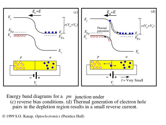
Fig. 2.37 Energy-band diagram of P–N junction diode with reverse bias V r with an increase in built-in potential E 0 and the width of the space charge region. Energy-Band Diagram for P–N diode with Reverse Bias. If V is negative and ≫ V T, then the current through the device, I = ...

Pn junction energy band diagram
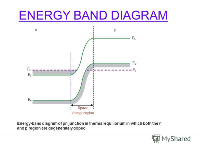
An energy diagram for a pn junction at the instant of formation is shown in Figure (a). As you can see, the valence and conduction bands in the n region are at lower energy levels than those in the p region, but there is a significant amount of overlapping. The free electrons in the n region that occupy the upper part of the conduction band in ... The Fermi level lies close to the conduction band in n-type material and it is close to valence band in p-type material. When a p-n diode is made with ... For a p-n junction at equilibrium, the fermi levels match on the two sides of the junctions. Electrons and holes reach an equilibrium at the junction and form a depletion region.The upward direction in the diagram represents increasing electron energy. That implies that you would have to supply energy to get an electron to go up on the diagram, and supply energy to get a hole to go down.
Pn junction energy band diagram. Consider that a PN junction has P-type and N-type materials in close physical contact at the junction on an atomic scale. Hence, the energy band diagrams of ...3 pages Fig:1.2.1 PN Diode Energy Band Diagram. (Source :https://ecee.colorado.edu). To reach thermal equilibrium, electrons/holes close to the metallurgical ...2 pages In solid-state physics of semiconductors, a band diagram is a diagram plotting various key electron energy levels as a function of some spatial dimension, ... Simplified energy band diagram of a p-n junction (a) at equilibrium ...
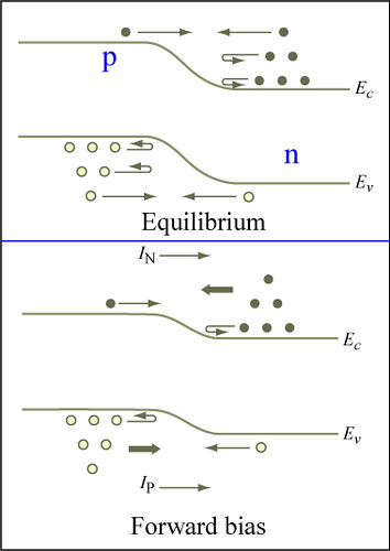
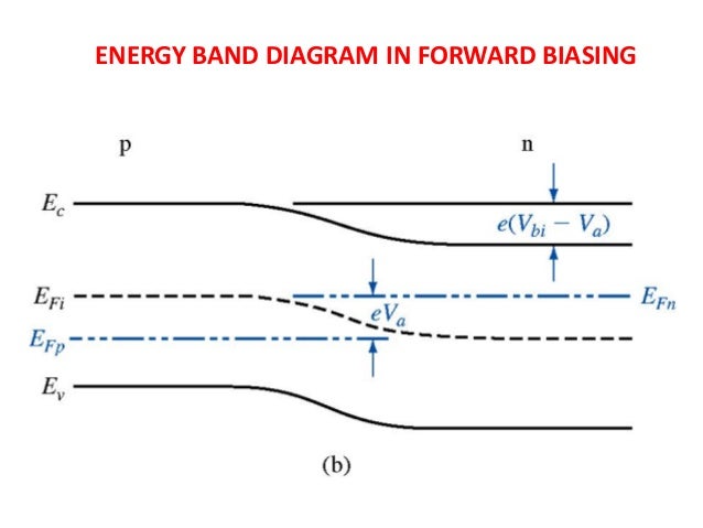
When a p-n junction is forward biased then its energy-band diagram looks like this: What would happen if V a > V b i? ( V b i is the built-in potential and V a is the externally applied voltage). Apparently, the bands would "reverse", in the sense that the conduction band limit in the p-side will be lower that the conduction band limite in the ... An energy diagram for a pn junction at the instant of formation is shown in Figure (a). As you can see, the valence and conduction bands in the n region are at lower energy levels than those in the p region, but there is a significant amount of overlapping. The free electrons in the n region that occupy the upper part of the conduction band in ... In a p on n structure, this can be accomplished by inserting an electron-blocking unipolar barrier at the junction of the pn diode to form the pBn diode (Klipstein, 2008). Figure 1.12 shows the reverse bias energy band diagrams of a pn diode and a pBn diode, calculated using heterojunction drift-diffusion simulation (Daniel et al., 2000). This quick video will give you a complete analysis of energy band diagram of pn juction diode. This quick video will give you a complete analysis of energy band diagram of pn juction diode.
q a i p p N n e φ0 ≈ = Energy =qV = ... On the band diagram, it would look like this: 10 Department of EECS University of California, Berkeley EECS 105 Spring 2004, Lecture 19 Prof. J. S. Smith Quasi-Fermi levels: Band edge diagram ... bi N P n p kT q n n kT q φ ... For a p-n junction at equilibrium, the fermi levels match on the two sides of the junctions. Electrons and holes reach an equilibrium at the junction and form a depletion region.The upward direction in the diagram represents increasing electron energy. That implies that you would have to supply energy to get an electron to go up on the diagram, and supply energy to get a hole to go down. The Fermi level lies close to the conduction band in n-type material and it is close to valence band in p-type material. When a p-n diode is made with ... An energy diagram for a pn junction at the instant of formation is shown in Figure (a). As you can see, the valence and conduction bands in the n region are at lower energy levels than those in the p region, but there is a significant amount of overlapping. The free electrons in the n region that occupy the upper part of the conduction band in ...
(a) Energy band diagram of isolated p-type Si and n-type ...
Miirbe: Pn Junction Band Diagram Forward Bias

Energy Band Structure Of Pn Junction Diode
15 The Energy Band Diagram Of A Pn Junction, In Wh ...
5: Abrupt p-n junction in thermal equilibrium adapted from ...

Energy band diagram for the tunnel diode showing the range ...

The energy band diagram of Au/α-PbO 2 /p-Si/Al ...
The Physics and Thermal Characterisation of Sharp LEDs ...

The pn-junction

Miirbe: Energy Band Diagram Of Pn Junction Diode

1: Formation of the p-n solid-state rectifying junction ...

P/N Junctions and Band Gaps

Energy-band diagram of a silicon p-n junction solar cell ...

p-n junction and its energy band diagram at equilibrium ...

4: Energy band diagram of a p - n junction Energy of the ...

Pn- Junction : Previous Year's Questions - DronStudy.com

Energy Band Diagram Of Pn Junction Diode Ppt

2: (a) Energy band diagram of a p-n junction doped with N ...

Equilibrium energy band diagram of the p-n heterojunction ...
2D pn junctions driven out-of-equilibrium - Nanoscale ...

The energy band diagram a, space charge distribution b ...

diodesymb.t

P-N Junction | Diagrams of p-n junction energy bands ...

Energy band diagram of the p + n +-homojunction ...
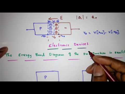
Electronic Devices Lecture-35: The Energy Band Diagram of ...
P-N Junction | Diagrams of p-n junction energy bands ...

Pn Junction Valence Band

Fig. S5: Energy band diagram during operation of a pn ...
P n junction--eema

Energy Band Diagram Of P N Junction Diode - Lessons - Tes ...
Презентация на тему: "Unit-2 JUNCTION DIODE ...

Energy band diagram in forward bias and reverse bias for a ...
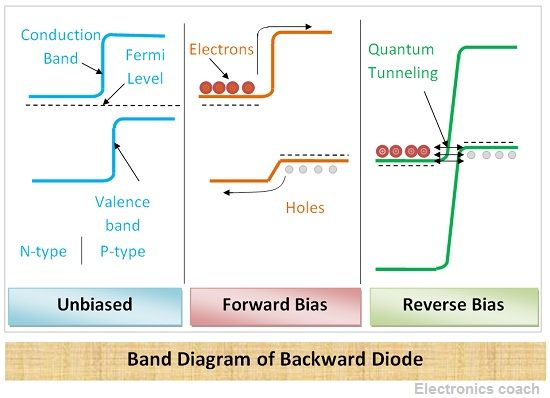
What is Backward Diode ? - Structure, Working, Advantages ...

3. PN Junction — Semiconductor Devices 1.0 documentation

Pn- Junction : Previous Year's Questions - DronStudy.com

Exam 2 at city college of san francisco - StudyBlue
Ete411 Lec14
What is the energy band diagram of an open circuited diode ...

Solved: Energy Band Diagram Of A Si P-n Junction Diode Is ...
.png)
Energy Band Structure Of Pn Junction Diode
0 Response to "40 pn junction energy band diagram"
Post a Comment